Electronics
One Day Builds - Day 2 - Enigma Machine Emulator
I went to Bletchley Park last week for a fascinating day trip. Bletchley Park was the location where the British code breakers were based during World War II. It was from here that Alan Turing and many other incredibly gifted mathematicians, statisticians, and translators worked tirelessly throughout the war to continuously crack and decrypt the messages sent by the Germans. During the war the Germans used several variants of an electro-mechanical rotatory cipher machine known as the Enigma machine. The Germans believed the encryption generated by these machine to be unbreakable. Theoretically there were in the order of 1.07 x 10^23 possible combinations for the Wehrmacht (Army) version of the machine. Fortunately (for the Allied forces) a weakness in the encryption method could be exploited and using a clever technique, alongside a custom build electro-mechanical device known as the Bombe, the message could be decrypted. To learn a bit more about how the Enigma machine worked I decided to make an Enigma Machine Emulator in C. Click here to see the code on GitHub. When I have more time I will update this page with lots more information about how the Enigma Machine works. |
One Day Builds - Day 1 - FPGA Pong
Since I hardly ever post anything to this website I've decided to submit a few projects in a slightly different format. At the moment every time I have a day free to do some electronics the thought of fully documenting the project and posting it on here puts me off! Instead, from now on, I'm going to do a series of one day builds where I have a singe day (or less) to make a specific project. I'll use this website like a lab book, documenting my progress as I go along. The notes will be rough but there should be enough detail to follow what I've done. I hope someone finds them useful/interesting. Build Log10:45 Research VGA interface and timing specifications There are 5 main signals for VGA:
H sync and V sync tell the monitor where the horizontal and vertical lines begin and end. See diagram below for details:  11:30 Work out timings for my monitor The timings of VGA signals depends on the desired resolution and refresh rate. My monitor has a native resolution of 1680 x 1050 resolution and supports a 60Hz refresh rate. VGA timings can be a bit awkward to calculate so it is often easier just to look them up online. I used this site which has a large selection of common resolutions. 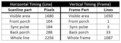 The horizontal width in pixels = "Front porch" width + "Sync pulse" width + "Back porch" width + monitor width. For my chosen resolution is 104 + 184 + 288 + 1680 = 2256. The vertical width in pixels is = "Front porch" width + "Sync pulse" width + "Back porch" width + monitor width. For my chosen resolution is 1 + 3 + 33 + 1050 = 1087. The h_sync line should be normally high, and then pulsed low for 184 pixels to trigger the h_sync. The v_sync line should be normally low, and then pulsed high for 3 pixels to trigger the v_sync. To get a refresh rate of 60Hz I need a pixel clock of 147.14MHz. This is calculated from: h_width * v_width * refresh rate = 2256 * 1087 * 60 = 147136320Hz 12:00 Start writing the VHDL I'm going to use my Altera DE1 development board as it has a VGA connector already on the board. The DE1 has a 4 bit DAC for each colour channel. So there are only 16*16*16 possible colours. This should be plenty for simple games like Pong. First I wrote a simple component in VHDL to count through each of the pixels in a line and then each of the lines in a frame. I also added some logic to generate the v sync and h sync pulses. The DE1 development board has a 50MHz oscillator. To get the required pixel clock frequency of 147.14MHz I used a Phased Locked Loop (PLL). The FPGA on the DE1 has 4 PLLs built in. The closest the PLL could get to 147.14MHz with a 50MHz reference was 147.22MHz which should be close enough. The refresh rate will just be slightly faster than 60Hz. 12:30 First test I set the FPGA to output a red box covering the whole visible area of the screen. The vertical alignment on the screen was perfect, but the horizontal was shifted to the right by about ~100 pixels making the right part of the image off the screen and the left of the screen black.  I did a few tests drawing small boxes on the screen at the limits of visibility. As initially thought the vertical alignment was fine, but the horizontal was shifted to the right. 12:45 Realised that I had mixed up the polarity of both the h_sync and v_sync pulses. Not sure why the vertical still seemed to work though. Fixed this and it worked! Next I tested with a 10 pixel line going around the edge of the screen. This would show up any alignment issues.  Seems to display perfectly with none of the image overlapping the edge of the screen. 13:15 Back after lunch. Time to make Pong! I uploaded the initial VGA driver code to github (GIST actually because it's only a small project) It can be found here. I rearranged the VHDL VGA component to allow other modules to write to the screen. Otherwise everything would have to be done within the VGA driver component. I decided to leave the 10 pixel boarder surrounding the screen as it makes it clear where the edge of the play area is. I quickly made a process to draw the paddles to the screen. The DE1 only has 3 buttons, I would need 4 to allow 2 players to move the paddle up and down. Instead I used the switches. If the switch is in the up position it moves the paddle upwards and vice versa. 14:37 Things are moving on the screen! Paddles are now moving based on the position of the switches. The paddles are also restricted from moving past the top and bottom of the screen.  I got the ball bouncing off the walls correctly. If it hits the top or bottom the vertical direction is reversed. Currently if it hits the left or right the horizontal direction is reversed. This will be changed to reset the ball and increment the score. I've set the velocity as an integer in VHDL. This means the speed could be increased gradually as the game progressed (not yet implemented). 15:30 It works Added the some very shoddy collision detection. Works by detecting when the FPGA is outputting both red and blue. Since only the paddles are red and only the ball is blue if both red and blue are outputted then a collision has occurred. When a paddle collision is detected the horizontal direction of the ball is reversed. 15:57 Playing pong against myself Collision detection works surprisingly well. Will probably leave it like this for the moment. Still need to add scoring and implement a reset when someone looses. Pushed code changes to GitHub. 16:30 Finalising the code Set the ball to reset when it hits the left or right side. Added scoring from 0 to 9 for each player, after which the game stops. Added 2 seven segment displays to show the score for each player. Cleaned up code and added a few more comments.  17:05 Done! I had a quick look at adding a PS/2 keyboard to the FPGA. It looked pretty easy, but then I realised that my keyboard is USB only. I pushed latest code to GitHub. All done for the day. I'll probably use the VGA driver in some future projects, maybe VGA Tetris... |
Beginners guide to I2C
I2C (or I2C) is a synchronous, half-duplex, serial, communication protocol commonly used to communicate between several integrated circuits on a PCB. I2C is often used to interface between a microcontroller and devices such as temperature sensors, accelerometers, and EEPROMs. The are two different types of I2C devices, master devices and slave devices. The master controls the I2C bus and sends commands to slave devices on the bus. Slave devices respond to commands from the master. Both master and slave devices can transmit and receive data, however only the master device can initiate a communication event. In most situations there is a single master on an I2C bus, while there can be many slave devices. It is possible to have multiple master devices on an I2C bus, however this is not that common and is outside the scope of this article. Physical interface I2C communication uses two wires, SDA (Serial data line) and SCL (Serial clock line). I2C devices connect to the bus in parallel as shown in the diagram below. 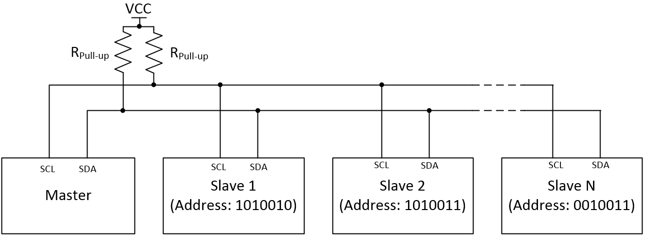 I2C devices use open drain outputs for both the SDA and SCL lines. This means that each device can either pull the line low, or allow it to float. When in the floating state pull up resistors are used to pull the voltage of the line up to VCC. The reason for using open drain outputs is that it prevents two devices on the bus from trying to force the line to both VCC and GND at the same time, which would cause a short circuit. The value for the pull up resistors is typically a trade off between the rise time of the signal and the current draw of the bus. A common choice is 4.7kOhms. If the I2C lines are long or there are many devices on the bus the capacitance of the I2C bus can be high. In order to meet signal rise time requirements the pull up resistance can be reduced (Tau = R*C). As a rule of thumb start around 4.7kohms and reduce the resistance gradually if that doesn't work. I2C addressing Each I2C device has a 7 bit address meaning there are 127 possible addresses (Although some are reserved for special purposes). The address of each device on the bus must be unique. The address of an I2C device is typically set by the manufacturer. Unfortunately there are tens of thousands of different I2C devices available so many devices have conflicting addresses. To get around this some devices allow several of the address bits to be set by connecting pins on the I2C device to VCC (1) or GND (0). The I2C specification also allows for 10 bit addresses, however these are not as common and are outside the scope of this article. If two devices with conflicting non user settable addresses must be used then either two separate I2C buses are required, or each IC must be enabled only when required via a chip select pin (like in SPI communications). I2C protocol When the I2C bus is idle both SDA and SCL are HIGH. When a master device wishes to start a communication event it first pulls SDA LOW and then after pulls SCL LOW. This special sequence is known as a start condition and lets all devices on the bus know that the bus is now in use. The stop condition tells all devices that communication is complete and the bus is now free. The stop condition occurs when the master allows the SDA line to go HIGH when the SCL line is already HIGH. The start and stop conditions are shown in the diagram below.  With the exception of the start and stop conditions all other changes of the SDA line occur only when SCL is LOW. Data is clocked into devices on the rising clock edge. The clock (SCL) signal is generated by the master device. Almost all I2C devices support clock speeds up to 100kHz, many support up to 400kHz, and some can go as high as 3.4MHz. I2C communications transmits data in 8 bit chunks. After the start condition has been set the master device transmits the address of the device it wishes to communicate with. Since the addresses are 7 bits long the address is shifted to the left and the least significant bit it set to either a 0 or 1 depending on if the master device wishes to read (1) or write (0) to the slave device. This is shown in the example below. 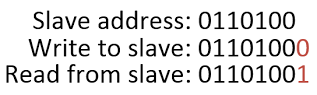 After each byte of data is transmitted, the receiving device acknowledges that it received the data and that the communications should continue. The acknowledge takes place on the 9th rising clock edge. The master allows the SDA line to float HIGH. If the slave has successfully received the data it pulls the line LOW, this is known as an ACK. If the slave is not present or is unable to process the data the line is left HIGH, this is known as a NACK (negative/no acknowledge). Write to slave The sequence of events required to write a single byte of data to a slave device are shown below:
The example below shows a master writing a byte of data (11101110) to a slave with address 0110100.  If multiple bytes of data are to be written to the slave then steps 4 and 5 are repeated until all the desired data is transferred. Read from slave The sequence of events to read data from a slave are shown below.
The example below shows a master reading a single byte of data from a slave with address 0110100. The slave replies with data 11101110 and the master replies back with a NACK indicating that it only wants this one byte of data.  I2C devices with registers Unfortunately most I2C devices are a little more complex to communicate with. These devices have several registers which can all be written and/or read from. Each register is assigned a memory address within the device. When communicating with these devices it is necessary to first write the address of the desired register to the I2C device. This sets the address pointer to the location of the desired register. Data can then be read or written to the device as previously explained. In most devices the address pointer automatically increments after each read or write. This means that when accessing sequential registers the address pointer only needs to be set once. Below is an example of a register map for an I2C temperature sensor. 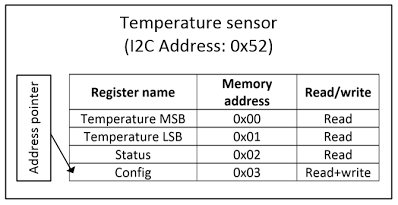 The sequence of events for writing to a specific register within a slave are shown below.
Reading a specific register on a slave The sequence of events for reading a specific register within a slave are shown below.
The diagram below shows the sequence of events for reading and writing to a typical I2C slave. Click on the image to see it full screen.  Real example Below is an example of a singe byte read from an ADT7410 I2C temperature sensor. The I2C address of the device is: 1001011 (0x4B). The address of the register being read is 0x0B which is the ID register for the ADT7410 sensor. The sensor replies with the data 0xCB.  Clock stretching Since the master controls the clock signal, it could attempt to try and read or write data to the slave when the slave is not ready. To overcome this issue the I2C specification includes a technique known as clock stretching. This is where a slave that has been asked to receive or transmit data can hold the clock (SCL) LOW until it is ready to continue. This indicates to the master that the slave is not ready and it will hold off sending the clock pulses until the slave releases SCL. Please note that not all I2C devices support clock stretching. Data ready notification There are many cases where a slave might need to let a master know that it has data ready to be read. There is no specific method for achieving this however two common method are:
General call The I2C address 0000000 (0x00) is reserved as a general call address. This allows all devices that respond to the general call to be communicated with at the same time. An example use for the general call is to synchronise several ADCs on an I2C bus to take a measurement at the same time. Please see the full I2C specification for more information on the general call. Recap
|
Cheap LED torch repair
 After waiting 3 weeks the torch finally arrived. The torch appeared to be mechanically well made, however after inserting the battery it became clear that it did not work. Considering the cost this was hardly surprising. I decided to take the torch apart to see how it worked and what was wrong with it.   The soldering on the board wasn't great, but everything seemed to be connected OK.  Using the continuity tester on a multimeter I identified the torch's circuit layout. The schematic is shown on the left. I removed the LED and connected it to a 3V coin cell battery. The LED worked fine, meaning the issue was with the driver circuitry. With a battery connected I checked the voltages at various points on the circuit board. Unfortunately everything seemed fine indicating that it was likely to be the driver IC that was faulty. I noticed on the torch's Amazon page that it would also work with a 3.7V 14500 lithium ion cell. Since I didn't have one to hand, I tested it at 3.7V using a bench power supply. Unfortunately that didn't work either. I will probably just bodge a constant current driver circuit into the torch as I doubt I will be able to source a replacement CX2859 IC. As always, you get what you pay for! |
Bluetooth controlled LED flashing frisbee
 A few friends and I decided it would be a good idea to make a light-up Frisbee so we could continue playing with it after it became dark.
The first version featured 8 LEDs located around the edge of the Frisbee. Each LED was connected in parallel via a resistor to a small LiPo battery. This worked well and looked really good in the dark.
I decided to make a second version using a microcontroller so that the LEDs could be flashed in various patterns. Since I had several BLE112 Bluetooth Low Energy (BLE) modules left over from a previous project, I decided to make a Bluetooth controlled flashing Frisbee! Why...? because "Everything is better with Bluetooth" (Sheldon Cooper).
The BLE112 modules include a 8051 microcontroller which can be programmed using a propitiatory scripting language called BGScript. BGScript was created by Bluegiga, the manufactures of the BLE112 modules. BGScript works great for simple applications, so it was perfect for this project.
 As part of a previous project I had designed a small PCB to breakout the pins on the BLE112 module to through hole 0.1" headers. The PCB was 1.3" x 1.6" and manufactured by OSH Park. In the interest of hacking the Frisbee together quickly I decided to reuse this PCB as well.
The BLE112 module can be powered by a small 3V lithium coin cell battery. As long as not too many of the LEDs were on at any one time, I decided that a coin cell would be good enough to power the whole Frisbee.
Like with the first version I decided to stick to using 8 LEDs. Since the BLE112 has 21 GPIOs I just directly connected each LED to an output on the module. By the time you take in to account the internal resistance of the CR2032 battery I used, it was not necessary to use any resistors between the BLE112 and the LEDs.
The PCB was attached in the centre of the Frisbee with the battery mounted on top. This way the majority of the extra weight was located in the centre where it would not affect the Frisbee's performance too much. Holes for the LEDs were drilled evenly around the Frisbee and the LEDs were mounted using a push fit. I will probably add glue to them for extra stability.
 The Bluetooth module was configured to provide an 8 bit attribute that was writeable by any device connected to it. Changing the attribute value via a phone or tablet would allow changing the flashing pattern and speed. Setting the attribute to a number less than 100 would change the sequence to the one assigned to that number (Only a few sequences were programmed in, but many more could be added. Invalid sequences were just ignored). Setting the attribute to a value between 100 and 255 would set the speed of flashing; higher numbers provide longer delays between each flash.
In the interest of speed I didn't write a smartphone app to control the Frisbee. Instead I used Bluegiga's example android app to send the 8 bit control values.
The code for the BLE112 module can be found on GitHub here.
Below are a few more photos of the Frisbee in action!


 |
Using an HD44780 alphanumeric LCD screen
 Most screens use the following pin-out, however it is best to refer to the screen's datasheet if available.
The screen has 3 main control lines. RS, R/W, and Enable. The RS and R/W lines determine the operation of the screen, as shown in the table below.
The Enable line acts like a clock signal. To clock data in or out of the display the enable line should be set high for 1uS. The enable signal is registered on the falling edge. The screen has 8 data lines which are used to both read and write data to and from the display. The screen can also operate with 4 data lines, where only DB4, DB5, DB6, and DB7 are used. In this case DB0 to DB3 can be left unconnected. This article will only cover operation of the display using all 8 data lines. Setting up the display Once the display is connected to the microcontroller, it needs to be correctly configured before it can be used. There are several settings that configure how the display operates; these are set by issuing commands to the LCD. To send a command to the LCD the microcontroller must first check if the screen is busy. If the screen is busy it will ignore any commands sent to it. The pseudo code below shows how to check if the screen is busy. Set data lines as inputsSet R/W = 1Set RS = 0Set enable highWait 1uSSet enable lowRead DB7If DB7 is high then LCD busy, else if DB7 is low then LCD readyWait until the screen is not busySet data lines to outputsSet R/W = 0Set RS = 0Set the 8 data lines to the desired commandSet enable highWait 1uSSet enable lowA list of commands can be found in the table below. Command table
The dash "-" means that it doesn't matter if the data bit is a 1 or 0. A is an address bit. The remaining bit settings are shown in the table below.
To initialise the display we need to send several configuration commands as shown in the pseudo code below. Wait until the screen is not busySet data lines to outputsSet R/W = 0Set RS = 0Set data lines to: 00111000 //Send "Function set" command. Sets display to 8 wire mode, 2 lines and 5x8 dots.Set enable highWait 1uSSet enable lowWait until the screen is not busy Set data lines to: 00000110 //Send "Set entry mode" command. Shift cursor right after character, don't move screen.Set enable highWait 1uSSet enable lowWait until the screen is not busy Set data lines to: 00001100 //Send "Display on/off" command. Display off, cursor hidden, don't blink cursor.Set enable highWait 1uSSet enable lowControlling the display Now the screen has been configured, data can be written to the LCD display. By default the cursor starts in the top left hand corner of the screen. The pseudo code below shows how the text "HI" can be written to the screen. Wait until the screen is not busySet data lines to outputsSet R/W = 0Set R/S = 1Set data lines to 01001000 //ASCII code for "H"Set enable highWait 1uSSet enable lowSet data lines to 01001001 //ASCII code for "I"Set enable highWait 1uSSet enable lowWhen "H" is entered the cursor automatically moves one character to the right. This means that when "I" is entered it appears to the right of "H". If you were to keep entering more characters the cursor would eventually disappear off the edge of the screen. Characters will still be written to the LCD, but they will not be visible. This is because while the screen may only have space for 16 (or 8) characters on each line, the controller actually has space to store 80 characters in its memory. A map of the display's memory (DDRAM) is shown below for the 4 most common LCD sizes.  Click image to enlarge To set the position of the cursor use the "Set DDRAM address" command from the command table further up the page. The pseudo code below shows how the cursor position can be set. Wait until the screen is not busySet R/W = 0Set RS = 0Set data lines to: 10000000 //Set DDRAM address. Cursor to Row 1, column 1Set enable highWait 1uSSet enable lowWait until the screen is not busySet R/W = 0Set R/S = 1Set data lines to 01001000 //ASCII code for "H"Set enable highWait 1uSSet enable lowWait until the screen is not busySet data lines to outputsSet R/W = 0Set RS = 0Set data lines to: 11000000 //Set DDRAM address. Cursor to Row 2, column 1Set enable highWait 1uSSet enable lowWait until the screen is not busySet R/W = 0Set R/S = 1Set data lines to 01001001 //ASCII code for "I"Set enable highWait 1uSSet enable lowThis will print "H" on row 1 and a "I" underneath it. Using the "Cursor/Display shift" command (see table further up the page) the cursor or screen can be moved left or right by one position. If the display is shifted the DDRAM addresses that are visible will change. This is shown in the image below.  The shift of the display can be reset by sending the "Return home" command (see command table further up the page). Displaying symbols and other characters The display supports the standard ASCII codes for the numbers 0-9, letters a-z and A-Z, as well as most standard ASCII symbols such as !?(),. In addition to these, there are many extra symbols. The characters are stored in the CGROM (Character generator rom). The contents of the CGROM can vary depending on who manufactured the display, but most manufactures either use the European or Asian character set produced by Hitachi. These can be found on pages 17 and 18 of the HD44780 datasheet. The European character set is shown below. Using the table the character code for any character in the set can be identified.  Symbols are sent to the screen in the same way as normal characters, as shown below. Wait until the screen is not busySet data lines to outputsSet R/W = 0Set R/S = 1Set data lines to 10011000 //Code for a bell symbolSet enable highWait 1uSSet enable low Generating custom LCD characters Sometimes it is necessary to display characters that are not part of the default character set. The HD44780 has space for 8 custom characters (5x8 dots) which can be displayed on the screen. (For 5x10 dot displays please refer to page 19 of the Hitachi datasheet). Each character requires 8 bytes of data, one for each of the 8 lines. The 3 MSBs of each byte are ignored, with the remaining 5 bits setting whether the dots appears on or off in the symbol, this is shown in the image below.  The CGRAM address of the first line of each of custom characters is shown in the table below. The character code is also shown. This is the code used to display the symbol when it has already been stored in the CGRAM.
The pseudo code below shows how a custom symbol can be stored and then displayed on the LCD screen. Wait until the screen is not busy //NB. this has been omitted from the rest of this code for claritySet data lines to outputsSet R/W = 0Set RS = 0Set data lines to: 01000000 //Set the CGRAM address to line 1 of custom character 1Pulse enableSet R/W = 0Set RS = 1Set data lines to: 000 01110 //Write line 1 of the characterPulse enableSet data lines to: 000 11011 //Write line 2 of the characterPulse enableSet data lines to: 000 10001 //Write line 3 of the characterPulse enableSet data lines to: 000 10001 //Write line 4 of the characterPulse enableSet data lines to: 000 10001 //Write line 5 of the characterPulse enableSet data lines to: 000 10001 //Write line 6 of the characterPulse enableSet data lines to: 000 10001 //Write line 7 of the characterPulse enableSet data lines to: 000 11111 //Write line 8 of the characterPulse enableSet R/W = 0Set RS = 0Set data lines to: 1000 0000 //Set the DDRAM address to row 1, column 1Pulse enableAn excellent web interface for designing custom characters can be found at quinapalus.com. Interfacing an HD44780 LCD display with a PIC microcontroller If you wish to use the HD44780 display with a PIC 16 microcontroller I have written a library that implements most of the functions of the display. The code can be found here. TODO
|
Kindle 3 (Keyboard) Screen Replacement
 My Kindle's screen recently broke and unfortunately it was out of warranty (and it was probably my fault anyway!). While amazon did offer to sell me a new Kindle at a reduced price, I wanted to keep my old kindle due to its worldwide free 3G web browsing capability. I ordered a new screen from eBay for around £40. Changing the screen was pretty simple and took about 30 minutes. My Kindle's screen recently broke and unfortunately it was out of warranty (and it was probably my fault anyway!). While amazon did offer to sell me a new Kindle at a reduced price, I wanted to keep my old kindle due to its worldwide free 3G web browsing capability. I ordered a new screen from eBay for around £40. Changing the screen was pretty simple and took about 30 minutes. I made video of the process in case instructions would be useful for anyone. I meant to take lots of photos during the process, but I was a little pushed for time, hopefully what I did take will suffice. Remember you can click the images to see them in full size. Step 1: Remove the back cover. It is held in place with small plastic clips. Use a fingernail or a spudger tool to slowly undo each clip. Be careful not to apply too much force as you may damage the plastic.  Step 2: Remove the 2 screws holding the battery in place, and then remove the battery.  Step 3: Remove the 2 screws holding the 3G card in place and remove the 3G card. You can detach the aerial connector if you wish, but this is not required and can be a little fiddly.  NB: If your kindle is not a 3G model then remove the 3G card placeholder. I believe this is held in place with a weak adhesive. Step 4: Remove the 10 silver screws indicated in the picture below. Also remove the black connector marked in the picture below.   Step 6: Remove the 8 black screws holding the main circuit board in place, and then carefully remove the board by sliding it upwards and then lifting it out.  Step 7: Remove the 3 black screws holing the main chassis, and then carefully remove the chassis.  Step 8: Remove the damaged screen and replace with a new one. Step 9: Reassemble the device by working backwards through steps 7 to 1. It is a good idea to check that the screen works before clipping the back back on. |
Wireless transmitter and receiver test
I recently purchased a cheap wireless transmitter and receiver from Seeed Studio. The modules operate at 433MHz using amplitude shift keying (ASK). Unfortunately there was very little information about the devices available on the Seeed Studio website.  The modules do not perform any error correction or detection, however this can be implemented using a microcontroller. In order to check that the devices were working I put together a quick test setup using an arduino and a bus pirate. The transmitter was connected directly to the arduino. The transmitter's signal pin was connected to the TX (pin 1) pin on the arduino. The transmitter's VCC and GND pins were connected to the 5V and GND rails on the arduino. Code to send a simple test pattern was written, as shown below.  At the other end, the receiver was connected to the bus pirate. VCC and GND on the receiver were connected to the +5V and GND connections on the bus pirate. The signal pin was connected to the MISO pin on the bus pirate. The bus pirate communicates with a computer through a serial interface. By using a program such as Putty we can connect to the bus pirate in order to configure it. The bus pirate uses the following settings in putty:
Once connected to the bus pirate type "?" without the quotes to bring up a list of commands.  In out case we only want to use the bus pirate as a serial to USB converter. To enable this mode type "m" to select the mode, type "3" to select UART, type "5" to select 9600 baud, type "1" to select 8bits and no parity, type "1" to select 1 stop bit, type "1" to select idle 1 operation, and type "1" to select open drain operation. Once in UART mode type "(2)" to select the UART monitor. If the transmitter and receiver are working correctly data will start appearing on the screen. The video below shows the operation of the system. Overall the transmitter and receiver seem to be working well. I plan to use them to create a wireless temperature logger. I will use a PIC microcontroller at both the transmitting and receiving ends of the system, in order to process, encode, and decode the data. My next step is to implement some form of error correction, probably using block coding. |
| Attachments:
![]() serial_test.ino
serial_test.ino
Operational Amplifiers - Ideal Circuits
If you are not familiar with op-amps it might be worth reading the first two articles in this series: Operational Amplifiers - Basic Concepts and Operational Amplifiers - Negative Feedback Ideal op-amp rules In the last article in this series it was shown that op-amps have a very large gain; when looking at ideal op-amps this gain is considered to be infinite. When put in a negative feedback configuration this infinite gain effectively means that the op-amp will drive the output to what ever value is necessary to make the voltage difference between the two inputs (V+ and V-) equal to zero. In addition to infinite gain two further assumptions are made when thinking about ideal op-amps. Firstly the input impedance of the amplifier's inputs is assumed to be infinite. This means that no current enters the op-amp's input terminals. In reality a small bias current is drawn. Secondly the output impedance of the op-amp is assumed to be zero. This means that the load connected to the op-amp's output terminal has no effect on the output voltage of the op-amp. In reality the output impedance of an op-amp is small but greater than zero. The three rules are summarised below: RULE 1: The op-amp will drive the output so that the voltage difference between the two inputs is zero. RULE 2: No current is drawn by the op-amp's inputs. RULE 3: The output load does not affect the op-amp's output voltage. Using the three rules we can develop several ideal op-amp circuits. The two most common op-amp circuits are the inverting amplifier and the non-inverting amplifier. Non-inverting amplifier The non-inverting amplifier applies a positive gain to the input. The configuration of a non-inverting amplifier is shown in figure 1 below.  Figure 1 The gain of the amplifier can be calculated using the three idea op-amp rules. It can be seen that the resistors R1 and R2 form an potential divider between Vout and GND. The output of the potential divider is at the negative input of the op-amp (called VA in figure 1). From this we can say that:  For example setting R2 to be 9 kohms and R1 to 1 kohms would give a gain of 10. It should be noted that the gain can not be set below 1 in this configuration. If R2 is a short circuit and R1 is an open circuit then the gain is 1. This called a buffer amplifier and was shown in the previous article. Inverting amplifier The inverting amplifier applies a negative gain to the input. The configuration of an inverting amplifier is shown in figure 2 below.  Figure 2  Since R2 and R1 are positive values the gain will always be negative. Differential amplifier A differential amplifier amplifies the difference between the two input terminals of the op-amp. The configuration of a differential amplifier is shown in figure 3.  Figure 3  If the resistors are set so that Rg/R2 = Rf/R1 then equation 10 cancels down to:  Summary This article has covered three ideal op-amp circuits, the non-inverting amplifier, the inverting amplifier and the differential amplifier. Methods to calculate the gains of each of these circuits have been shown.
The next article will cover several further idea op-amp circuits. |
Operational Amplifiers - Negative Feedback
If you are not familiar with op-amps it might be worth reading the first article in this series: Operational Amplifiers - Basic Concepts. Closing the loop - Negative feedback The first article in this series only looked at the open loop configuration of an op-amp, while this has its uses, most applications require some form of feedback. In a closed loop system some part of the system's output is fed back to the input. Figure 1 below shows a closed loop op-amp circuit. In this image beta represents the transfer function applied to the feedback path.  Figure 1 can be re-drawn so that it is easier to visualise, as shown in Figure 2.  In this diagram A(OL) is the open loop gain of the op-amp, which is typically assumed to be greater than 100,000. Using Figure 2 the gain transfer function for the system can be derived:   It can be seen from equation 6 that the closed loop gain is only dependant on the feedback path from the amplifier, and not the open loop gain. This is very useful since a precise value for the open loop gain is not something that is normally known. Example - Voltage follower So how does it all work? Let's take the simplest example of an op-amp configured as a voltage follower (also called a buffer amplifier). This is where the closed loop gain is set to 1 by directly connecting the output to the inverting input (V-). This is shown in figure 3 below.  If a 1V step increase is applied to V(IN) the output voltage will rise as a result of the amplifier gain. This rise in output voltage causes a rise in the feedback voltage, which acts to decrease the differential voltage between the V+ and V- inputs. The system quickly stabilises at point were V+ is roughly equal to V-. In most circuit application it is fine to say that V+ is so close to V- that they are essentially equal. Ideal op-amp equations make the assumption that the gain of the amplifier is infinite, if this was true then the difference between V+ and V- would actually be 0V. In the interest of fully understanding how the system operates it is useful to know how it works in the real world. As previously mentioned the gain of the amplifier is not infinite, however it can be assumed to be very large, say 100,000. Also if the differential voltage between V+ and V- was really 0V the output of the amplifier would also be 0V. As a result the difference between V+ and V- must be large enough that when multiplied by the amplifier gain it produces an output voltage roughly equal to V(IN). For example if V(IN) is set to 1V and the open loop gain of the amplifier A(OL) = 100,000 we can use equation 5 to calculate the actual gain. Closed loop gain A(CL) = A(OL)/( 1+Beta*A(OL) ) = 100,000/(1+1*100,000) = 0.999990000099999 From this the expected output voltage can be calculated: V(out) = Vin * A(CL) = 1*0.999990000099999... = 0.999990000099999...V In a voltage follower V- = V(out), therefore the differential voltage between V+ and V- = 1 - 0.999990000099999... = 9.99990000099999...uV (NB. I have used ... to indicate that the sequence continues) It can be see that this tiny differential voltage is enough for the amplifier to generate the desired 1V output, or at least very close to it! As mentioned previously this example was more to help with understanding the concept, it is rare that it is necessary to do these calculations for a real situation, especially since many op-amps have much larger gains than 100,000. Summary This article has covered the use of negative feedback with op-amps. It is also possible to use positive feedback (I.e the feedback loop connected to the non-inverting input) however this will be covered in a future article.
The next article covers ideal op-amp circuits using negative feedback, including the inverting and non-inverting amplifier circuits. Click here to proceed to the next article in the series: Operational Amplifiers - Ideal Circuits |
1-10 of 12